Custom-made MIT tool probes materials at nanoscale
Offers advantages to researchers across many disciplines
An MIT physicist has built a new instrument of interest to MIT researchers across a wide range of disciplines because it can quickly and relatively inexpensively determine a variety of important characteristics of a material at the nanoscale. It’s capable of not only determining internal properties of a material, such as how that material’s electrical or optical conductivity changes over exquisitely short distances, but also visualizing individual molecules, like proteins.
“Modern materials research has greatly benefited from advanced experimental tools,” says Long Ju, an assistant professor in the Department of Physics. Ju is an expert on an emerging instrument that combines nanoscopy—the ability to see things at the nanoscale—with spectroscopy, which probes materials by exploring their interactions with light.
The tool, known as near-field infrared nanoscopy and spectroscopy (it is also known as Scattering-type Scanning Nearfield Optical Microscopy, or s-SNOM) is available commercially. However, “it’s rather challenging for new users, which limits the applications of the technique,” says Ju.
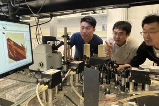
So the Ju group built its own version of the tool—the first s-SNOM at MIT—and in May completed a second, more advanced version with additional functions. Now both instruments are available to the MIT community, and the Ju group is on hand to provide assistance to MIT users and to develop new functionalities. Ju encourages MIT colleagues to contact him with potential applications or questions.
“It’s exciting because it’s a platform that can in principle host many different materials systems and extract new information from each,” says Ju, who is also affiliated with MIT’s Materials Research Laboratory. “It’s also a platform for some of the best minds in the world—MIT researchers—to conceive things beyond what can be done on a standard s-SNOM.”
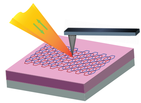
The new tool is based on atomic force microscopy (AFM), in which an extremely sharp metallic tip with a radius of only 20 nanometers, or billionths of a meter, is scanned across the surface of a material. AFM creates a map of the physical features, or topography, of a surface, of such high resolution that it can identify “mountains” or “valleys” less than a nanometer in height or depth.
Adding Light
Ju is adding light to the equation. Focusing an infrared laser on the AFM tip turns that tip into an antenna “just like the antenna on a television that’s used to receive signals,” he says. And that, in turn, greatly enhances interactions between the light and the material beneath the tip. The backscattered light collected from those interactions can be analyzed to reveal much more about the surface than would be possible with a conventional AFM.
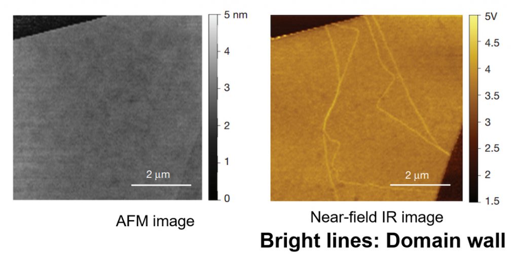
The result: “you can get an image of your sample with three orders of magnitude better spatial resolution than that of conventional infrared measurements,” says Ju. In earlier work reported in Nature, he and colleagues published images of graphene taken with AFM and with the new tool. There are features in common between the two, but the near-field image is riddled with bright lines that are not visible in the AFM image. They are domain walls, or the interfaces between two different sections of a material. Those interfaces are key to understanding a material’s structure and properties.
Images of similar detail can be captured with transmission electron microscopy (TEM), but TEM has some drawbacks. For example, it must be operated in an ultra-high vacuum, and samples must be extremely thin for suspension on a film or membrane. “The former limits the experimental throughput, while the latter is not compatible with most materials,” says Ju.
In contrast, the near-field nanoscope “can be operated in air, does not require suspension of the sample, and you can work on most solid substrates,” Ju says.
Many Applications
Ju notes that the near-field tool can not only provide high-resolution images of heights; the analysis of backscattered light from the machine’s tip can also give important information about a material’s internal properties. For example, it can tell metals from insulators. It can also distinguish between materials with the same chemical composition but different internal structures (think diamond versus pencil lead).
In an example he describes as “especially cool,” Ju says that the instrument could even be used to watch a material transition from insulator to superconductor as the temperature is changed. It is also capable of monitoring chemical reactions on the nanoscale.
Ju also notes that the new tool can be operated in different ways for different purposes. For example, he said, the tip of the tool can either be scanned across a surface while being irradiated with a set wavelength of light, or the tip can be parked over a certain area and probed with light of different wavelengths. Different wavelengths of light interact differently with different materials, giving even more information about a given material’s composition or other characteristics.
Ju, who came to MIT in 2019, is thoroughly enjoying meeting other MIT researchers who might have applications for his machine. “It’s exciting to work with people from different research areas. You can work together to generate new ideas at the cutting edge.”
This work is sponsored by MIT’s Materials Research Laboratory.