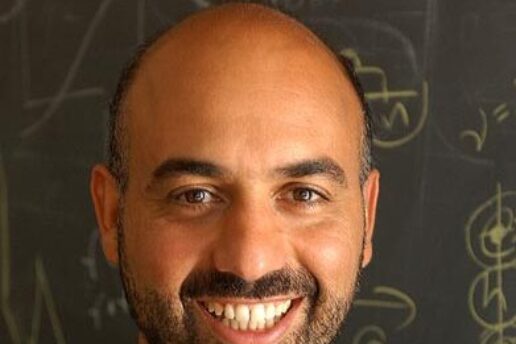
Faculty highlight: Raymond Ashoori
Novel experimental technique reveals exotic behaviors in graphene systems.
The process of scientific discovery often results from hard work and good luck in the lab rather than from theoretical predictions, MIT physics professor Raymond C. Ashoori says.
“A lot of the physics that we do arises from serendipity and luck, and we have interesting tools to [bring to] bear on an interesting system,” Ashoori says. “Let’s see what we see. It’s very rare for me actually to say there is this particular thing I want to test and to study it. Generally, the techniques that we have are pretty different from the commonly used measurements. In a lot of cases, we just don’t know what we’re going to see.”
One technique that took Ashoori more than a decade to develop is time domain capacitance spectroscopy (TDCS), a pulse tunneling method that can send on the order of a million short electrical pulses through a material to study its electronic properties. Until recently, Ashoori’s group has focused on using TDCS on semiconductor samples, but they now see an exciting possibility for work in graphene.
Semiconductor systems have been a key focus of Ashoori’s research. Ashoori’s group at MIT recently demonstrated a unique bandgap in graphene coupled to hexagonal boron nitride that could be a precursor to developing the material for functional transistors. The work was a collaboration with Pablo Jarillo-Herrero, the Mitsui Career Development Associate Professor of Physics at MIT, and other researchers in Japan and Arizona.
“In most materials, electrons behave as though they have a mass,” Ashoori says. “In graphene, they look like they don’t have a mass. They look like they’re behaving like photons. This is good and bad. It means electronic properties of graphene are really different. For instance, it becomes hard to make barriers to impede their flow. You can’t make transistors that you can actually turn off completely, because these massless electrons can get through the barriers that you try to put in their way. But if you have an energy gap and massive electrons, then you can actually create transistors that you can turn off.”
Recent research in the collaboration between Ashoori and Jarillo-Herrero showed that having a component of the applied magnetic field in the graphene plane forced electrons at the edge of graphene to move in opposite directions based on their spins.
“What we were able to have happen and to see was that at the edges of this piece of graphene, electrons with one spin move in one direction, and electrons with the opposite spin move in the opposite direction,” Ashoori says. “It’s the kind of thing that you would naturally want for lots of spintronic devices. You could use them in various kinds of spin filters.”
Because of the very high magnetic fields and very low temperatures used, the recent studies aren’t directly applicable to room-temperature semiconductor systems such as computers. Says postdoctoral fellow Benjamin M. Hunt, who was coauthor of papers on both the bandgap and the spin polarized electron work, “The exact system that we’re studying is probably not applicable; however, the physical principles that we are unveiling may be applicable to a system that you can study at much higher temperatures and much lower magnetic fields, something that might be attainable someday at room temperature. It’s really the physical principles that we’re interested in exposing.” Hunt notes that Jarillo-Herrero was an equal contributor to both papers.
Ashoori is also a co-principal investigator for the Center for Integrated Quantum Materials, a five-year project funded by the National Science Foundation and based at Harvard University. “With our group at MIT, we’re all thinking about very similar kinds of problems,” Ashoori says. “It’s a pretty tight fit.” (See related article.)
Technique-driven research
Ashoori’s research is often driven by novel experimental techniques. “What excites me most is seeing a new kind of signal, a new kind of measurement, and that’s where the pulse tunneling for me was really exciting,” Ashoori says. “Nothing like it exists anywhere else. Right now, there is no other place doing it besides our lab, and there is no other measurement that gives you the same information, so it’s a pretty unique thing.” The technique applies on the order of a million electric pulses, each about 100 nanoseconds in duration, and measures currents during those times.
The research is carried out in dilution refrigerators that operate near absolute zero temperature, which poses its own set of challenges. “Right now we have an amplifier in our dilution fridge that operates with a few microwatts of power, and it has a gain of two-thirds, but that’s what was required to make the thing work,” Ashoori says.
With postdoc coauthors Andrea Young and Ben Hunt interviewing this year for faculty positions, Ashoori hopes that they’ll take the group’s experimental techniques to other places and create a community of people doing similar research. (See related article.)
“With this tunneling technique, we can look at what is called the single particle spectrum of these materials, which is just asking, ‘If I try to inject an electron, will it go in at this energy, is there room for it, and how much room is there for it?’” Ashoori says. It can also reveal the probability that an electron will move to a sample, and how much energy that will take.
“We’ve studied the two-dimensional electron system a lot, and people have tried to look at it optically, but it turns out the optical spectrum is often difficult to interpret. What we’re doing is much simpler. We’re really asking, can this system accept an electron at this energy, period. And that spectrum is a lot simpler to understand than a lot of other ones. It’s a very direct way of getting at a lot of basic physics in these systems. That has been a main thrust for us, and we were lucky enough to get funding from the Moore Foundation.”
While the technique has focused largely on semiconductor sample analysis, Ashoori hopes to make it into a much broader technique. “Imagine that you can have any little object, and you don’t have to have electrical contact, you just have to be able to place a tunnel barrier on top of it, and then you determine the energies required for adding electrons to the object and also observe the single particle spectrum — the likelihood that an electron can enter the object at a particular energy,” he says. “The recent advances in creating and placing exfoliated thin layers of boron nitride and other insulators mean that we can place thin tunnel barriers on top of just about any objects on a surface that we might want to study.”
The Ashoori group’s capabilities for making sensitive capacitance measurements were a key to the findings in the recent work on graphene. “In those studies, the capacitance measurements that we made showed the development of energy gaps in those systems,” Ashoori says. “We could sense directly that we were seeing results from having massive fermions, such as electrons, instead of massless ones, which ordinarily is what you have in graphene.”
Serendipitous finding
In a two-dimensional system like graphene — a flat single-atom-thick layer of carbon atoms arranged in a hexagonal lattice pattern — electrostatic potential at any carbon atom is identical to the one next to it. This “sublattice symmetry” results in electrons behaving as if they have no mass. By stacking the graphene on a similarly patterned layer of boron nitride, the researchers found that interactions between carbon and boron atoms on one sublattice and carbon and nitrogen atoms on the other resulted in adequate breaking of the sublattice symmetry to give the electrons an observable mass.
Adjacent identical carbon atoms in the graphene lattice are referred to as A sites and B sites. “If I’m on an A site or a B site and my potential energy is the same, then the electron will have no mass,” Ashoori says. “If I can make those two sites different, the A sites and the B sites, then the electron can have a mass. So that’s what we do. You make them different.”
“We studied many samples and we didn’t see this, we weren’t really looking for it, but what happened was there is this underlying material, boron nitride, which has a very similar structure to graphene, except its A sites and B sites have different energy potential,” Ashoori says.
Still, this only happens in about 1 out of 15 samples when the hexagonal lattices of graphene and boron nitride are in near perfect alignment. Even within those nearly perfectly aligned samples, the alignment will vary across a layer because the lattice spacing in the boron nitride is slightly larger than that of carbon, meaning that as you move farther from a point of alignment, the overlapping lattices will go out of register at other points. “Let’s say I make the A sites higher potential than the B sites, and let’s say I call that positive mass,” Ashoori says. “Due to the difference in lattice constants between the two materials, this reverses at some other position, so the A sites would be lower potential than the B sites, and then the math ends up calling that negative mass. Between the regions of positive and negative mass, there is a boundary where mass equals zero. The thing that is harder to understand is that, despite this expected variation of mass with position, the mass that we measure is close to the maximum mass, rather than the average of zero.”
“A dream in graphene is that you could make transistors that you could turn off,” Ashoori says. “And to make transistors that you can turn off, you need that gap. And in creating the gap, at the same time, we get particles that behave like they have mass, so the two things go hand in hand.”
“The size of the gap that we have is about 30 millivolts,” Ashoori says. “If you translate that to temperature, it’s about 300 degrees Kelvin, which is room temperature. It turns out that to make a room-temperature device that you could turn off, you want that gap to be 10 times bigger. So rather than being 300 Kelvin, it would be nice to have it be 3,000 Kelvin, so you could really shut it off. We’re not there yet. That’s something where if we find a way to enhance the gap just another order of magnitude, then we might be in business.”
Collaborative effort
The graphene-boron nitride work grew out of a collaboration with Jarillo-Herrero’s group, which had expertise in building and measuring stacks of graphene and boron nitride and other layered materials. Ashoori’s postdoctoral fellow Hunt and Jarillo-Herrero’s graduate student Javier Sanchez-Yamagishi made samples with those layering techniques. Young added fabrication techniques he learned as a graduate student at Columbia in the group of Professor Philip Kim, who is moving to Harvard. All three worked together on the measurements. “We ended up having this dream team of really highly qualified people working together,” Ashoori says.
“I think things are often still just discovered rather than predicted, and sometimes you can discover things that actually had been predicted and you didn’t realize they had been,” Ashoori says. “I find it really fun to not know what’s going to happen. Our work is really geared up toward exploration.”
RELATED LINKS